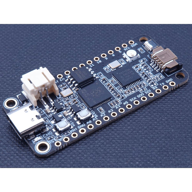
The Challenger RP2040 NFC is a small embedded computer, equipped with an advanced on-board NFC controller (NXP PN7150), in the popular Adafruit Feather form factor. It is based on an RP2040 microcontroller chip from the Raspberry Pi Foundation which is a dual-core Cortex-M0 that can run on a clock up to 133 MHz. NFC The PN7150 is a full featured NFC controller solution with integrated firmware and NCI interface designed for contactless communication at 13.56 MHz. It is fully compatible with NFC forum requirements and is greatly designed based on learnings from previous NXP NFC device generation. It is the ideal solution for rapidly integrating NFC technology in any application, especially small embedded systems reducing Bill of Material (BOM). The integrated design with full NFC forum compliancy gives the user all the following features: Embedded NFC firmware providing all NFC protocols as pre-integrated feature. Direct connection to the main host or microcontroller, by I²C-bus physical and NCI protocol. Ultra-low power consumption in polling loop mode. Highly efficient integrated power management unit (PMU) allowing direct supply from a battery. Specifications Microcontroller RP2040 from Raspberry Pi (133 MHz dual-core Cortex-M0) SPI One SPI channels configured I²C Two I²C channel configured (dedicated I²C for the PN7150) UART One UART channel configured Analog inputs 4 analog input channels NFC module PN7150 from NXP Flash memory 8 MB, 133 MHz SRAM memory 264 KB (divided into 6 banks) USB 2.0 controller Up to 12 MBit/s full speed (integrated USB 1.1 PHY) JST Battery connector 2.0 mm pitch On board LiPo charger 450 mA standard charge current Dimensions 51 x 23 x 3,2 mm Weight 9 g Note: Antenna is not included. Downloads Datasheet Quick start example
Specificaties
Dubbele ARM Cortex-M0+ @ 133 MHz
264 kB on-chip SRAM in zes onafhankelijke banken
Ondersteuning tot 16 MB off-chip Flash memory via speciale QSPI bus
DMA-controller
Volledig aangesloten AHB crossbar
Interpolator en integer divider peripherals
On-chip programmeerbare LDO om spanning voor de core te genereren
2x on-chip PLL's om USB en core kloksignalen te genereren
30x GPIO pins, waarvan er 4 als analoge ingangen kunnen worden gebruikt
Randapparatuur
2x UARTs
2x SPI controllers
2x I²C controllers
16x PWM kanalen
USB 1.1 controller en PHY, met host en device support
8x PIO state machines
Wat je krijgt
10x RP2040 ICs
The FRDM-MCXN947 is a compact and versatile development board designed for rapid prototyping with MCX N94 and N54 microcontrollers. It features industry-standard headers for easy access to the MCU's I/Os, integrated open-standard serial interfaces, external flash memory, and an onboard MCU-Link debugger.
Specificaties
Microcontroller
MCX-N947 Dual Arm Cortex-M33 cores @ 150 MHz each with optimized performance efficiency, up to 2 MB dual-bank flash with optional full ECC RAM, External flash
Accelerators: Neural Processing Unit, PowerQuad, Smart DMA, etc.
Memory Expansion
*DNP Micro SD card socket
Connectivity
Ethernet Phy and connector
HS USB-C connectors
SPI/I²C/UART connector (PMOD/mikroBUS, DNP)
WiFi connector (PMOD/mikroBUS, DNP)
CAN-FD transceiver
Debug
On-board MCU-Link debugger with CMSIS-DAP
JTAG/SWD connector
Sensor
P3T1755 I³C/I²C Temp Sensor, Touch Pad
Expansion Options
Arduino Header (with FRDM expansion rows)
FRDM Header
FlexIO/LCD Header
SmartDMA/Camera Header
Pmod *DNP
mikroBUS
User Interface
RGB user LED, plus Reset, ISP, Wakeup buttons
Inbegrepen
1x FRDM-MCXN947 Development Board
1x USB-C Cable
1x Quick Start Guide
Downloads
Datasheet
Block diagram
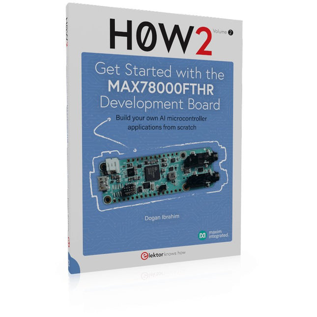
Build your own AI microcontroller applications from scratch
The MAX78000FTHR from Maxim Integrated is a small development board based on the MAX78000 MCU. The main usage of this board is in artificial intelligence applications (AI) which generally require large amounts of processing power and memory. It marries an Arm Cortex-M4 processor with a floating-point unit (FPU), convolutional neural network (CNN) accelerator, and RISC-V core into a single device. It is designed for ultra-low power consumption, making it ideal for many portable AI-based applications.
This book is project-based and aims to teach the basic features of the MAX78000FTHR. It demonstrates how it can be used in various classical and AI-based projects. Each project is described in detail and complete program listings are provided. Readers should be able to use the projects as they are, or modify them to suit their applications. This book covers the following features of the MAX78000FTHR microcontroller development board:
Onboard LEDs and buttons
External LEDs and buttons
Using analog-to-digital converters
I²C projects
SPI projects
UART projects
External interrupts and timer interrupts
Using the onboard microphone
Using the onboard camera
Convolutional Neural Network
The Challenger RP2040 WiFi is a small embedded computer equipped with a WiFi module, in the popular Adafruit Feather form factor. It is based on an RP2040 microcontroller chip from the Raspberry Pi Foundation which is a dual-core Cortex-M0 that can run on a clock up to 133 MHz. The RP2040 is paired with a 8 MB high-speed flash capable of supplying data up to the max speed. The flash memory can be used both to store instructions for the microcontroller as well as data in a file system and having a file system available makes it easy to store data in a structured and easy to program approach. The device can be powered from a Lithium Polymer battery connected through a standard 2.0 mm connector on the side of the board. An internal battery charging circuit allows you to charge your battery safely and quickly. The device is shipped with a programming resistor that sets the charging current to 250 mA. This resistor can be exchanged by the user to either increase or decrease the charging current, depending on the battery that is being used. The WiFi section on this board is based on the Espressif ESP8285 chip which basically is a ESP8266 with 1 MB flash memory integrated onto the chip making it a complete WiFi only requiring very few external components. The ESP8285 is connected to the microcontroller using a UART channel and the operation is controlled using a set of standardized AT-commands. Specifications Microcontroller RP2040 from Raspberry Pi (133 MHz dual-core Cortex-M0) SPI One SPI channel configured I²C One I²C channel configured UART One UART channel configured (second UART is for the WiFi chip) Analog inputs 4 analog input channels WLAN controller ESP8285 from Espressif (160 MHz single-core Tensilica L106) Flash memory 8 MByte, 133 MHz SRAM memory 264 KByte (divided into 6 banks) USB 2.0 controller Up to 12 MBit/s full speed (integrated USB 1.1 PHY) JST Battery connector 2.0 mm pitch Onboard LiPo charger 250 mA standard charge current Onboard NeoPixel LED RGB LED Dimensions 51 x 23 x 3,2 mm Weight 9 g Downloads Datasheet Design files Product errata
Build your own AI microcontroller applications from scratch
The MAX78000FTHR from Maxim Integrated is a small development board based on the MAX78000 MCU. The main usage of this board is in artificial intelligence applications (AI) which generally require large amounts of processing power and memory. It marries an Arm Cortex-M4 processor with a floating-point unit (FPU), convolutional neural network (CNN) accelerator, and RISC-V core into a single device. It is designed for ultra-low power consumption, making it ideal for many portable AI-based applications.
This book is project-based and aims to teach the basic features of the MAX78000FTHR. It demonstrates how it can be used in various classical and AI-based projects. Each project is described in detail and complete program listings are provided. Readers should be able to use the projects as they are, or modify them to suit their applications. This book covers the following features of the MAX78000FTHR microcontroller development board:
Onboard LEDs and buttons
External LEDs and buttons
Using analog-to-digital converters
I²C projects
SPI projects
UART projects
External interrupts and timer interrupts
Using the onboard microphone
Using the onboard camera
Convolutional Neural Network
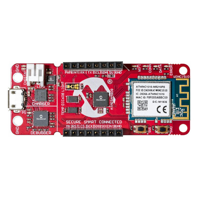
The AVR-IoT WA development board combines a powerful ATmega4808 AVR MCU, an ATECC608A CryptoAuthentication™ secure element IC and the fully certified ATWINC1510 Wi-Fi network controller – which provides the most simple and effective way to connect your embedded application to Amazon Web Services (AWS). The board also includes an on-board debugger, and requires no external hardware to program and debug the MCU.Out of the box, the MCU comes preloaded with a firmware image that enables you to quickly connect and send data to the AWS platform using the on-board temperature and light sensors. Once you are ready to build your own custom design, you can easily generate code using the free software libraries in Atmel START or MPLAB Code Configurator (MCC).The AVR-IoT WA board is supported by two award-winning Integrated Development Environments (IDEs) – Atmel Studio and Microchip MPLAB X IDE – giving you the freedom to innovate with your environment of choice.Features
ATmega4808 microcontroller
Four user LED’s
Two mechanical buttons
mikroBUS header footprint
TEMT6000 Light sensor
MCP9808 Temperature sensor
ATECC608A CryptoAuthentication™ device
WINC1510 WiFi Module
On-board Debugger
Auto-ID for board identification in Atmel Studio and Microchip MPLAB X
One green board power and status LED
Programming and debugging
Virtual COM port (CDC)
Two DGI GPIO lines
USB and battery powered
Integrated Li-Ion/LiPo battery charger
Dit carrier bord combineert een 2.4' TFT scherm, zes adresseerbare LED's, on-board spanningsregelaar, een 6-pins IO-connector, en microSD slot met het M.2 pin connector slot zodat het kan worden gebruikt met compatibele processorborden in ons MicroMod ecosysteem. We hebben dit carrier board ook uitgerust met Atmel's ATtiny84 met 8kb programmeerbare flash. Deze kleine jongen is voorgeprogrammeerd om met de processor te communiceren en via I2C druktoetsen te lezen. Eigenschappen M.2 MicroMod Connector 240 x 320 pixel, 2.4' TFT display 6 Addresseerbare APA102 LEDs Magnetische Buzzer USB-C Connector 3.3 V 1 A spanningsregelaar Qwiic Connector Boot/Reset toetsen RTC Backup Batterij & laadcircuit microSD Kruiskopschroef M2.5 x 3 mm meegeleverd
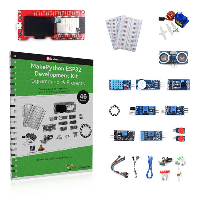
Leer hoe je de ESP32 Microcontroller en het programmeren met MicroPython in je toekomstige projecten kunt gebruiken!
Het (Engelstalige) projectboek, geschreven door de bekende Elektor auteur Dogan Ibrahim, bevat vele software- en hardware-gebaseerde projecten die speciaal voor de MakePython ESP32 ontwikkelkit ontwikkeld zijn. De kit wordt geleverd met verschillende LED's, sensoren, en actuatoren. De kit helpt je de basiskennis op te doen om eigen IoT projecten te maken.
Alle volledig geëvalueerde projecten in het boek zijn voorzien van de bijgeleverde componenten. Elk project bevat een blokschema, een schakelschema, een volledige programmalijst, en een volledige programma beschrijving.
Inbegrepen in de kit
1x MakePython ESP32 ontwikkelingsboard met LCD
1x Ultrasone afstandsmeter
1x Temperatuur- en luchtvochtigheidssensor
1x Zoemer module
1x DS18B20 module
1x Infrarood module
1x Potentiometer
1x WS2812 module
1x Geluidssensor
1x Trilsensor
1x Module met lichtgevoelige weerstand
1x Puls sensor
1x Servo motor
1x USB kabel
2x Knop
2x Breadboard
45x Schakeldraad
10x Weerstand 330R
10x LED (Rood)
10x LED (Groen)
1x Projectboek (Engelstalig, 206 pagina's)
Boek met 46 projecten
LED Projecten
Knipperende LED
SOS knipperende LED
Knipperende LED – met behulp van een timer
Afwisselend knipperende LEDs
Knopbediening
De knippersnelheid van de LED's veranderen met drukknop onderbrekingen
Chasing-LEDs
Binaire teller met LEDs
Kerstverlichting (willekeurig-knipperende 8 LEDs)
Elektronische dobbelsteen
Geluksdag van het week
Projecten voor Pulsewidth Modulation (PWM)
Genereer een PWM golfvorm van 1000 Hz met 50% duty cycle
LED helderheid regelen
Meten van de frequentie en duty cycle van een PWM golfvorm
Melodieën maker
Eenvoudig elektronisch orgel
Servo motor besturing
Servo motor DS18B20 thermometer
Projecten voor analoog naar digitaal converteren (ADC)
Voltmeter
Plotten van de analoge ingangsspanning
Interne temperatuursensor van de ESP32
Ohmmeter
Lichtgevoelige weerstandsmodule
Projecten voor digitaal naar analoog converteren (DAC)
Opwekken van vaste spanningen
Opwekken van een zaagtand-golf signaal
Opwekken van een driehoek-golf signaal
Golfvorm met willekeurige periode
Genereren van een sinus-golf signaal
Genereren van een nauwkeurig sinus-golf signaal met behulp van een timer interrupts
Gebruik van het OLED Display
Seconden teller
Gebeurtenisteller
DS18B20 digitale thermometer met OLED
ON-OFF temperatuur regelaar
Meten van temperatuur en luchtvochtigheid
Ultrasone afstandsmeting
Hoogte van een persoon (stadiometer)
Hartslag (polsslag) meten
Andere bij de set geleverde sensoren
Diefstal alarm
Met geluid geactiveerd licht
Infrarood obstakel-vermijding met zoemer
WS2812 RGB LED ring
Tijdregistratie van temperatuur en luchtvochtigheid
Netwerkprogrammering
Wi-Fi scanner
Bediening op afstand vanuit de Internet browser (met een smartphone of PC) – Webserver
Temperatuur- en luchtvochtigheidsgegevens opslaan in de Cloud
Werking met Low-Power
Gebruik een timer om de processor te laten ontwaken
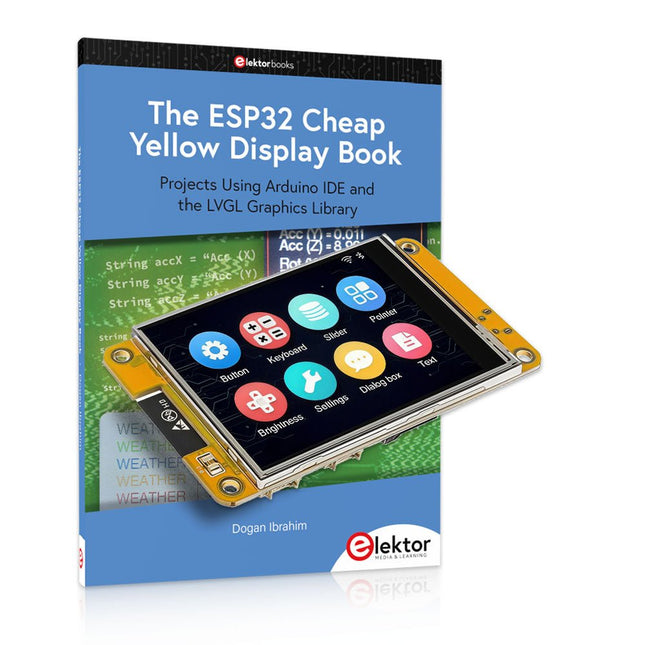
Meer dan 40 volledig geteste ESP32-projecten met Arduino IDE en de LVGL grafische bibliotheek
Deze bundel bevat de ESP32 Cheap Yellow Display (CYD) – een compact ontwikkelbord dat een standaard ESP32-microcontroller combineert met een TFT-kleurendisplay van 320 x 240 pixels. Het bord beschikt ook over meerdere aansluitingen voor GPIO, seriële communicatie (TX/RX), voeding en aarde. Het ingebouwde display is een groot voordeel, omdat gebruikers hiermee complexe, grafische projecten kunnen maken zonder dat er externe LCD's of displays nodig zijn.
Het bijbehorende boek introduceert de hardware en de ingebouwde aansluitingen van het CYD-bord in detail. Het biedt een reeks projecten van beginners- tot gevorderdenniveau, ontwikkeld met de populaire Arduino IDE 2.0. Zowel basis grafische functies als de krachtige LVGL grafische bibliotheek worden behandeld, met praktische projecten die elke aanpak illustreren.
Alle meegeleverde projecten zijn volledig getest en klaar voor gebruik. Het boek bevat blokdiagrammen, circuitschema's, complete codelijsten en stapsgewijze uitleg. Met de LVGL-bibliotheek kunnen lezers moderne, kleurrijke grafische interfaces maken met behulp van widgets zoals knoppen, labels, schuifregelaars, kalenders, toetsenborden, grafieken, tabellen, menu's, animaties en meer.
ESP32 Cheap Yellow Display Board
Dit ontwikkelbord (ook bekend als "Cheap Yellow Display") wordt aangedreven door de ESP-WROOM-32, een dual-core MCU met geïntegreerde Wi-Fi- en Bluetooth-mogelijkheden. Het werkt op een hoofdfrequentie tot 240 MHz, met 520 KB SRAM, 448 KBROM en 4 MB Flash-geheugen. Het bord is voorzien van een 2,8-inch scherm met een resolutie van 240 x 320 en resistieve aanraking.
Bovendien bevat het bord een achtergrondverlichtingsbesturingscircuit, aanraakbesturingscircuit, luidsprekeraandrijfcircuit, lichtgevoelig circuit en RGB-LED-besturingscircuit. Het biedt ook een TF-kaartsleuf, seriële interface, DHT11 temperatuur- en vochtigheidssensorinterface en extra IO-poorten.
De module ondersteunt ontwikkeling in Arduino IDE, ESP-IDE, MicroPython en Mixly.
Toepassingen
Beeldoverdracht voor Smart Home-apparaat
Draadloze bewaking
Slimme landbouw
Draadloze QR-herkenning
Signaal van draadloos positioneringssysteem
En andere IoT-toepassingen
Specificaties
Microcontroller
ESP-WROOM-32 (Dual-core MCU met geïntegreerde Wi-Fi en Bluetooth)
Frequentie
Tot 240 MHz (rekenkracht is maximaal 600 DMIPS)
SRAM
520 KB
ROM
448 KB
Flash
4 MB
Bedrijfsspanning
5 V
Stroomverbruik
ca. 115 mA
Display
2,8" TFT-kleurenscherm (240 x 320)
Touch
Resistief Touch
Driver chip
ILI9341
Afmetingen
50 x 86 mm
Gewicht
50 g
Downloads
GitHub
Inhoud van de bundel
The ESP32 Cheap Yellow Display Book (normale prijs: € 35)
ESP32 Cheap Yellow Display Board (normale prijs: € 25)
1x ESP32 Dev Board met 2,8" display en acryl-behuizing
1x Touchpen
1x Aansluitkabel
1x USB-kabel
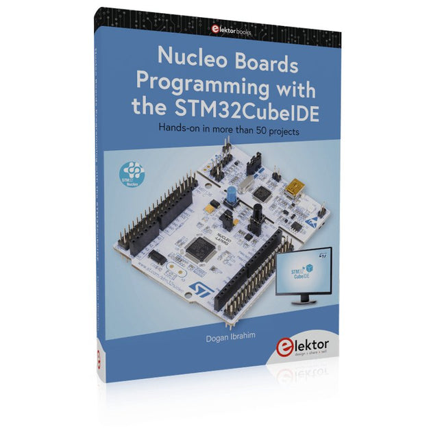
Hands-on in more than 50 projects
STM32 Nucleo family of processors are manufactured by STMicroelectronics. These are low-cost ARM microcontroller development boards. This book is about developing projects using the popular STM32CubeIDE software with the Nucleo-L476RG development board. In the early Chapters of the book the architecture of the Nucleo family is briefly described.
The book covers many projects using most features of the Nucleo-L476RG development board where the full software listings for the STM32CubeIDE are given for each project together with extensive descriptions. The projects range from simple flashing LEDs to more complex projects using modules, devices, and libraries such as GPIO, ADC, DAC, I²C, SPI, LCD, DMA, analogue inputs, power management, X-CUBE-MEMS1 library, DEBUGGING, and others. In addition, several projects are given using the popular Nucleo Expansion Boards. These Expansion Boards plug on top of the Nucleo development boards and provide sensors, relays, accelerometers, gyroscopes, Wi-Fi, and many others. Using an expansion board together with the X-CUBE-MEMS1 library simplifies the task of project development considerably.
All the projects in the book have been tested and are working. The following sub-headings are given for each project: Project Title, Description, Aim, Block Diagram, Circuit Diagram, and Program Listing for the STM32CubeIDE.
In this book you will learn about
STM32 microcontroller architecture;
the Nucleo-L476RG development board in projects using the STM32CubeIDE integrated software development tool;
external and internal interrupts and DMA;
DEBUG, a program developed using the STM32CubeIDE;
the MCU in Sleep, Stop, and in Standby modes;
Nucleo Expansion Boards with the Nucleo development boards.
What you need
a PC with Internet connection and a USB port;
STM32CubeIDE software (available at STMicroelectronics website free of charge)
the project source files, available from the book’s webpage hosted by Elektor;
Nucleo-L476RG development board;
simple electronic devices such as LEDs, temperature sensor, I²C and SPI chips, and a few more;
Nucleo Expansion Boards (optional).
Onboard each moto:bit are multiple I/O pins, as well as a vertical Qwiic connector, capable of hooking up servos, sensors and other circuits. At the flip of the switch, you can get your micro:bit moving! The moto:bit connects to the micro:bit via an updated SMD, edge connector at the top of the board, making setup easy. This creates a handy way to swap out micro:bits for programming while still providing reliable connections to all of the different pins on the micro:bit. We have also included a basic barrel jack on the moto:bit that is capable of providing power to anything you connect to the carrier board. Features More reliable Edge connector for easy use with the micro:bit Full H-Bridge for control of two motors Control servo motors Vertical Qwiic Connector I²C port for extending functionality Power and battery management onboard for the micro:bit